How to design a CPU in two deceptively simple steps
Why is this Hardware meme funny?
Level 1: First Brick, Then a House
Imagine someone gave you a two-step guide on how to build a house. Step 1 says: “Lay down one brick.” Okay, that seems easy. 🧱 Step 2 then says: “Now build the rest of the entire house.” 🏡 See the problem? Building a whole house isn’t just one brick and one quick step – it’s thousands of bricks, plus wiring, plumbing, windows, a roof, and lots of careful work. You’d laugh at those instructions because they skip 99% of the actual work needed and just say “do the rest.”
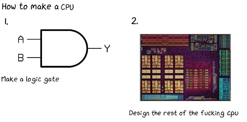
That’s exactly why this meme is funny. It’s doing the same thing, but with a computer chip (a CPU) instead of a house. The first picture says “make a logic gate,” which is like the tiniest piece of a computer’s brain – kind of comparable to that one brick. The second picture basically says “now make the entire CPU,” which is like “now build the whole house.” The joke is pointing out how absurd it is to treat something incredibly complicated as if it were super simple.
If you’ve ever tried to do a big project and someone made it sound way easier than it really was, you can feel the humor here. It’s that eye-rolling moment of, “Oh sure, is that all? Just everything else, huh?” The meme makes us laugh because we know that between the easy first step and the finished product, there’s a huge invisible journey of hard work – and pretending it’s “magical” or instantaneous is just silly. It’s a fun reminder that big things are built out of many, many small steps, even if the instructions forget to mention them.
Level 2: One Gate at a Time
Let’s break this down more straightforwardly. In digital electronics, a logic gate is a tiny electronic circuit that takes one or more binary inputs (0s and 1s, representing false/true or off/on) and produces a binary output. The first panel shows an AND gate. This gate outputs 1 (true) only if both input A AND input B are 1; otherwise the output is 0. It's one of the basic building blocks of all digital systems (along with OR, NOT, etc.). In a schematic, we draw it as a kind of D-shaped symbol like in the meme, but physically, inside a chip, that gate would be made up of a few transistors (transistors are like tiny switches that implement the logic).
Now, a CPU (Central Processing Unit) is essentially the brain of a computer. It's the hardware that executes instructions and processes data. The CPU is built using many logic gates and other circuits working together. You can think of making a CPU as a huge Lego project: the logic gates are like individual Lego bricks. One brick by itself doesn't do much, but if you connect thousands or millions of them in clever ways, you can build very complex structures.
So, how do we get from a single gate to something as powerful as a CPU? We take a step-by-step, modular approach (at least in theory). For example, with just AND, OR, and NOT gates, you can build a circuit called a half-adder that adds two 1-bit numbers. It will output a sum bit and a carry bit (since 1 + 1 = 2, which in binary is 10). If you build several half-adders and link them, you get a full adder that can add multi-bit numbers (like 32-bit integers). This adder is a small part of what’s called an ALU (Arithmetic Logic Unit) – the component of the CPU that handles arithmetic (addition, subtraction) and logical operations. An ALU itself might use dozens of gates. Then you will have registers (which are essentially small memory storage elements made from flip-flops) to hold the current values the CPU is working with. Connect the ALU to some registers and you have a rudimentary datapath – data can flow from registers, through the ALU, and back into registers.
But a CPU needs to do more than one operation; it needs to follow a sequence of instructions (a program). This is where the control unit comes in. The control unit is a collection of circuits that send signals to all parts of the CPU to coordinate them. It’s kind of like an orchestra conductor making sure the right instruments (gates and sub-circuits) play at the right time. For example, when an instruction says “ADD A, B, and store in C”, the control logic will: ensure the value from register A and register B are fed into the ALU’s inputs; tell the ALU to perform an addition; then take the ALU’s output and write it into register C on the next clock pulse. This control logic can be implemented with state machines (think of it like a flowchart that moves step by step) or even a small embedded program inside the CPU (called microcode in some designs).
Now, a modern CPU is not just a single adder and a couple of registers, of course. There are many registers, multiple ALUs (to do operations in parallel), specialized units for things like floating-point math, instruction decoding logic (to interpret the binary instruction codes from a program), and more. And to make it run fast, the CPU will be pipelined – which means it has stages so it can work on several instructions at once (as mentioned above, like an assembly line). There will also be caches, which are small on-chip memories that store frequently used data and instructions to speed things up. And if the CPU has multiple cores (which many do), then essentially it’s like having several mini-CPUs on one chip, which introduces the need for them to coordinate (especially regarding memory – hence the cache coherence we touched on).
The second panel is showing a die shot. That’s basically a photograph or render of the actual silicon chip of a CPU after it's manufactured (with the protective packaging removed). In a die shot, different colors or regions indicate various components. For example, you might see symmetrical regions that correspond to CPU cores, large areas that could be caches, IO controllers, etc. If you look closely (or with annotation), you’d find that within each of those blocks are incredibly tiny features – those are the literally millions of transistors and wires. By contrast, the first panel’s AND gate diagram is very abstract and simple; it doesn’t show any physical detail. It’s as if panel 1 is saying “take this small unit,” and panel 2 is showing “now imagine this insanely complex chip with billions of those units inside – go make that”. The joke being that the second part is doing 99.999% of the work but is dismissed as just "the rest."
For someone early in their learning (say a computer science or electrical engineering student), the process of actually making a CPU might start in a simulator or a simple environment. They might write a description of a simple CPU in a hardware description language (HDL) like Verilog or VHDL. For instance, to describe an AND gate in Verilog, it’s literally one line of code:
// A simple 2-input AND gate in Verilog:
assign Y = A & B;
That’s it – one line to create the AND logic (as a combinational continuous assignment). However, describing an entire CPU would require thousands of lines of such code, stiches together. You'd define modules for the ALU, for the register file, for the control unit, etc., and wire them all. In a college project, your “CPU” might be something that can run a few simple instructions (like adding or moving numbers) and maybe fits on a small FPGA board or in a simulator. Even that is a significant project taking weeks or months for a beginner to get right!
Now, imagine scaling that up to a CPU that could run an actual operating system like Windows or Linux. You need it to handle perhaps hundreds of different instructions, interrupts (signals that pause normal execution to handle urgent tasks), interaction with memory and peripherals, and do it all reliably at high speed. At that point, it’s not just a learning exercise – it’s a full-blown engineering project. It requires knowledge of computer architecture (how to design the instruction set and overall structure), digital design (how to implement that with gates and finite state machines), and even some computer science fundamentals (like algorithms for branch prediction or cache management). This is why the meme resonates with low-level programming folks and hardware engineers: they know there’s an enormous amount of work hidden behind that breezy two-step “tutorial.”
When you see the text “Design the rest of the CPU” scrawled under the intricate chip image, it’s highlighting the hidden complexity. It’s saying, "Sure, step 1: do the easy part; step 2: now do the insanely complex part that we didn’t talk about." This kind of humor pops up in engineering because often outsiders (or even higher-level documentation) might trivialize a hard problem. If you’ve ever read an oversimplified guide or had someone tell you “oh, that’s easy, you just do X” when X is actually really challenging, you’ll get a chuckle from this.
In summary, panel 1 (the AND gate) represents the very beginning of building something – the simplest component. Panel 2 (the CPU die) represents the finished product at a complexity level that is hard to fathom when you're at the start. The gulf between them is huge. The meme humorously skips over that gulf and pretends it’s one quick jump. It’s funny to those in the know because it's a massive oversimplification – akin to saying you can build a skyscraper by first laying a brick and then “just building the rest of the skyscraper.” Anyone who’s tried a project of that scale, even on a smaller level like building their own little CPU, appreciates just how much is being swept under the rug with that joke.
Level 3: Insert Magic Here
This meme nails a very familiar joke in engineering: the oversimplified tutorial. In panel 1, we see step 1 of “How to make a CPU” – “Make a logic gate.” Sure, that’s technically the starting point: an AND gate with inputs A, B and output Y. But then panel 2 jumps to step 2, which, in a sudden burst of exasperation, says “Design the rest of the fucking CPU.” The humor lies in that huge, comical leap. It’s basically saying, “Oh, is that all? Just design everything else!”
For anyone who has worked in hardware or low-level systems, this resonates on multiple levels. First, it satirizes how tutorials or textbooks sometimes gloss over complexity. It reminds us of those “step-by-step” guides that start simple and then abruptly say “and now just do the complicated part” as if it's nothing. There's a classic nerd joke about a professor outlining a proof: Step 1: [something easy], Step 2: Then a miracle occurs, Step 3: Q.E.D.. Here, “Design the rest of the CPU” is that miracle step, delivered with a heavy dose of sarcasm. The inclusion of the swear word fucking in the caption is actually doing a lot of work comedically – it captures the exasperation of an engineer who's been through that pain. It’s as if the person writing the steps got to step 2, realized it encapsulates years of work, and just blurted out that frustrated line. Hardware engineers chuckle at this because they feel that exasperation: going from one simple gate to a whole CPU is not a single step, but more like a thousand very hard steps.
In real-world terms, after you “make a logic gate,” here's a glimpse of what that “rest of the CPU” entails (something a cheeky tutorial might hide under the rug):
- Define the ISA (Instruction Set Architecture) – You have to decide what instructions your CPU will support (add, subtract, load, store, jump, etc.), and how those instructions are represented in binary. This is like setting the vocabulary and grammar that both the hardware and any software running on it will speak.
- Build the ALU and datapath – The Arithmetic Logic Unit is the part of the CPU that performs operations like addition, subtraction, bitwise AND/OR (yes, built from many logic gates!). Alongside the ALU, you need a datapath: wires and multiplexers to route operands (data inputs) from registers or memory to the ALU and back. Even something as conceptually simple as adding two 32-bit numbers involves designing a chain of 32 one-bit adders with carry logic connecting them.
- Design the control unit – This is the “brain within the brain” that sequences steps for each instruction. It can be hardwired logic or microcode, but either way, it uses state machines built from gates or small ROMs. The control unit ensures that on cycle 1, the instruction is fetched; on cycle 2, it’s decoded; on cycle 3, the right signals are asserted so the ALU does its job, etc. If you have a pipeline, the control logic also has to handle pipeline hazards, flush the pipeline on a mispredicted branch, and so forth.
- Add pipelining and hazard handling – If you want your CPU to go faster, you pipeline it. That means breaking the work into stages and processing multiple instructions at once. But then you must deal with instructions that interfere with each other. For example, if one instruction writes to a register that the very next instruction needs, the naive pipeline will give the wrong result. Handling this might require stalling (pausing the pipeline for a cycle) or data forwarding (rerouting the result to where it’s needed instantly). And for branches (which alter the flow of instructions), you’ll incorporate a branch predictor to guess the next instructions and some logic to flush or fix the pipeline when the guess is wrong.
- Integrate memory and caching – A CPU without memory is useless. You need to design an interface to memory (which could be as simple as a bus protocol or as complex as a multilevel cache system). Most modern CPUs include on-chip caches: small, fast SRAM memories that keep copies of recently used data and instructions. Designing a cache involves choosing a size, a block (line) size, mapping scheme (direct-mapped? 2-way associative? fully associative?), and a replacement policy. And if your CPU is multi-core, now you have to ensure cache coherence so one core’s changes to a memory location become visible to others. Suddenly, you’re dealing with MESI protocol state machines and cache invalidation traffic between cores. Fun times!
- Verify and test – For every piece of logic you design, you need to verify it works. Professionals write extensive testbenches and use simulation tools to run the CPU design through countless scenarios. This might mean writing small assembly programs to test every instruction, every corner case (like does the ADD instruction set the zero flag correctly when the result is zero? what happens on arithmetic overflow? does the branch predictor recover properly on a loop or a function return?). Verification is often the lengthiest part of a hardware project — it’s not unheard of for verification engineers to outnumber design engineers. And even then, bugs can slip through, which is why companies also develop formal proofs for critical components or run massive randomized test patterns overnight.
- Physical design (place-and-route) – Once the logical design seems sound, there’s the task of translating it into a chip layout. That means placing millions of logic gates (actually, tiny transistor structures called standard cells) on a silicon canvas and wiring them up in metal layers. Tools attempt to optimize this for area (you want the chip smaller to reduce cost) and timing (wires have delay; long or too-thin wires can slow signals, so critical signals need short, thick routes or even duplicate drivers). The result of place-and-route is something like that colorful image in panel 2: a layout where every wire and transistor is precisely positioned. Engineers then do timing closure checks to ensure the placed design meets the target clock speed, and power analysis to ensure it doesn’t overheat or draw too much power. If problems arise, they might have to tweak the design (like change logic to balance pipeline stages or insert additional buffering).
- Firmware and boot code – Here’s a step many forget: once you have the hardware, you often need some low-level software (firmware) to get it running. For example, on reset, a CPU might start executing a predefined boot ROM code that brings the system to life (initializing registers, setting up memory controllers, etc.). In more complex CPUs, microcode might be used to implement certain instructions or handle faults. Designing a CPU thus also involves writing and testing this lowest-level software, which is very hardware-specific.
Each of those bullet points is a deep rabbit hole. Seasoned engineers reading them are probably nodding (or cringing) because they know each one breaks down into dozens more sub-tasks. For instance, “Verify and test” could involve test benches, simulation at the gate level vs. RTL level, FPGA prototyping, formal equivalence checks, etc. The meme humorously condenses months (or years) of work into that cheeky Step 2. It’s the same energy as saying: “Step 1: Boil some water. Step 2: Now create a five-course gourmet dinner.”
The reason this strikes a chord is that many of us have experienced the hidden complexity behind projects. Maybe you, as a junior developer or student, once thought writing a compiler or an operating system would be straightforward after reading the theory, only to discover the devil’s in the details. In hardware, that gap between theory and practice is enormous. In school, a professor might have you build a simple 8-bit CPU on an FPGA or simulate it in software as a semester project. It’s a tough but manageable project because they typically give you a blueprint (maybe a simplified MIPS or RISC-V design with a few hundred gates). But a commercial-grade 64-bit out-of-order superscalar CPU with caches and all? That’s the result of decades of collective experience and tool development. No single person can hold the entire design in their head.
Historically, this gap has widened. Early CPUs like the Intel 4004 (1971) had roughly 2,300 transistors and ran at 740 kHz; a determined engineer could design something like that almost single-handedly (and indeed, back then small teams built the first microprocessors). Today’s CPUs (2020-era and beyond) pack billions of transistors, run at several GHz, and incorporate features unimaginable in the 70s. It requires large teams and very specialized roles: one group focuses just on the branch predictor, another on the vector arithmetic units, another on the physical layout, another on validation, etc. Yet, the way we introduce people to this field is still by starting with that one simple logic gate or a basic adder. We kind of have to: you can’t present a freshman with a billion-transistor monster on day one. The education process must break it down into bite-sized pieces. But the result is that newcomers often underestimate how much remains to go from that first piece to the whole puzzle.
So the meme’s joke is a wink and a nudge. It says, “Sure, building a CPU is easy – first, do the easy part, and for the second step... well, just magically do everything else.” The absurdity is obvious and laughable, especially to those of us who have been in the trenches of a complex engineering project. It’s engineering humor encapsulating a universal truth: any sufficiently advanced project looks simple until you actually try to do it. That second panel’s caption, with its exasperated tone, is basically every senior engineer’s internal scream when someone trivializes their very hard work.
Level 4: Microarchitectural Magic
In theory, a CPU is nothing more than an enormous network of basic logic gates orchestrated to perform computations. But bridging that conceptual simplicity to a physical microarchitectural design is where the real magic lies. The meme’s first panel shows a humble two-input logic gate (an AND gate) — the kind of thing you might see on day one of a digital logic course. It’s true that at the lowest level, all digital circuits (CPUs included) reduce to combinations of Boolean functions like AND, OR, and NOT. In fact, you can build any computation using enough of these gates; they’re functionally complete. However, what's glossed over is the staggering leap from one gate to a full modern CPU. A processor isn’t just one gate repeated a billion times – it’s a carefully organized hierarchy of circuits and subsystems solving countless problems simultaneously.
Consider the pipeline in a modern processor: an assembly line where an instruction passes through multiple stages (fetch, decode, execute, memory access, write-back). Each stage is itself composed of many logic gates and registers clocked in unison. By overlapping these stages (while one instruction is being executed, the next is being decoded, and a third is being fetched, etc.), a CPU can vastly improve throughput. But this introduces complexity like pipeline hazards – what if an instruction needs the result of a previous one that's still in the pipeline? Engineers devise techniques like forwarding (aka bypassing) and stalling to handle these hazards. And that’s just for a simple in-order pipeline. High-performance CPUs go further with out-of-order execution, where instructions are dynamically reordered to avoid stalls. This requires sophisticated scheduling logic, issue queues, and reorder buffers to keep track of which instructions are in flight and to ensure the CPU eventually retires them in the correct order. Now add branch predictors into the mix: specialized circuits that guess the outcome of conditional branches (if/else decisions in code) so the CPU can speculatively execute ahead without waiting. A modern branch predictor might use a history of branch outcomes and complex pattern matching (e.g., two-level adaptive predictors, BTBs, etc.), and when it guesses wrong, the pipeline must be flushed and corrected – another burst of intricate logic to discard or commit results safely.
Then there’s the memory subsystem. Caches (L1, L2, L3...) are small, fast memories on the chip that store copies of frequently used data to hide the latency of main memory (RAM). Each cache isn’t just a plain memory array; it has tag directories to quickly check if a requested address is in the cache, and implements policies for eviction (like LRU – least recently used – replacement). In a multi-core CPU, caches introduce the need for cache coherence protocols (e.g. MESI or MOESI) to ensure each core sees a consistent view of memory. Designing and verifying those protocols is itself as complex as a full undergraduate course – one core invalidating a cache line in another, bus snooping or mesh interconnects, atomic memory operations... it’s a lot. And we haven’t even mentioned things like speculative execution side-effects, memory ordering (the subtleties of Intel's x86 total store ordering vs. weaker models), or fine-grained clock gating (turning off parts of the chip to save power when idle). Each of these concerns blooms into a sophisticated sub-architecture of its own.
All these logical components must be meticulously coordinated and timing-optimized. Real silicon runs on a clock; modern desktop CPUs tick billions of times per second (several GHz). That means every combinational logic path – from one register flip-flop, through some gates, into the next register – must settle to the correct value within a fraction of a nanosecond. Engineers perform exhaustive timing analysis and pipeline balancing to ensure no path is too slow (or the chip would have to run at a lower clock speed). They also wrestle with metastability and synchronization when crossing clock domains (e.g., when the CPU talks to peripheral devices on a different clock). And because so many transistors switching at once can draw huge currents, the chip needs carefully engineered clock distribution networks and power grids, plus strategies to manage heat (ever notice the elaborate cooling in PCs? CPUs can get hot when billions of transistors toggle).
Finally, turning a verified logical design into actual silicon is an entirely different kind of nightmare magic. The meme’s second panel – that colorful maze-like image – is a die shot of a real microprocessor, essentially a photograph of the chip's silicon layout under a microscope. Every colored block in that image represents countless transistors and wires forming functional units: arithmetic logic units, register files, cache arrays, decoders, and so on. Drawing a simple AND gate on a whiteboard is easy; laying out a billion transistors on a chip so that they all function correctly and efficiently is a task of epic proportions. Engineers use advanced Electronic Design Automation (EDA) tools for this phase: they write the design in a hardware description language (like Verilog or VHDL) at a high level (often called RTL – Register Transfer Level), then use logic synthesis tools to convert that RTL into a vast sea of gates. Next, place-and-route tools take over, figuring out how to physically place each of those millions of logic cells on the silicon die and route the metal interconnect wires between them. This is akin to solving a three-dimensional jigsaw puzzle with both logical and physical constraints – and it’s computationally hard (many aspects of chip layout are NP-hard optimization problems). The tools must obey rules about how close transistors can be, how wide wires must be to carry currents, how to minimize signal delay, and avoid crosstalk between neighboring signals. Often after an initial place-and-route, engineers find the design doesn’t meet timing or consumes too much area, and have to iterate: adjust the architecture or floorplan, tweak power distribution, maybe add pipeline stages or buffers – then run the tools again, a process that can take many hours or days for large chips.
Even after layout is finalized, the journey isn’t over. The design goes through verification steps at multiple levels of abstraction to ensure that this incredibly complex beast will actually work in practice. There’s formal verification for critical algorithms (for example, proofs that the cache coherence protocol maintains consistency), random test generation to poke at corner cases, and full-system simulations where you run actual software on a model of the chip. Engineers create testbenches and use simulation/emulation platforms to run billions of cycles of test patterns. The reason for this thoroughness? Once you commit that design to silicon (often called tape-out), it’s going to be manufactured onto wafers at a fabrication plant. If a bug is found after manufacturing, you can't just patch it easily – you might have to design a workaround or, in worst cases, scrap or re-spin the chip (which costs a fortune and time-to-market). The infamous Pentium FDIV bug in the 1990s (where a subtle flaw in the division hardware yielded incorrect math results) cost Intel hundreds of millions and a lot of public embarrassment. So modern CPU design teams are almost paranoid in verification. They even include extra circuits on the chip like scan chains and built-in self-test logic purely to help test each chip after manufacturing.
In summary, that funny jump from an AND gate to a fully realized CPU hides entire worlds of complexity. It spans theoretical computer science (logic design, automata for control), computer engineering (architecture and RTL design), and electrical engineering (circuit layout, signal integrity, semiconductor physics). The meme's humor comes from treating all of that like it's the easy part. The second panel’s detailed silicon die shot, with its maze of interconnects and functional blocks, is a testament to how much design and optimization goes into "the rest of the CPU." Microarchitectural design is equal parts engineering and wizardry: we start with basic logic gates, but it takes something close to magic (the hard-earned, methodical kind) to weave them into a modern processor.
Description
A two-panel meme humorously oversimplifying the process of creating a CPU, formatted like a 'how-to' guide. The title reads, 'How to make a CPU'. The first panel, labeled '1.', shows a simple black-and-white diagram of an AND logic gate with inputs A and B and output Y, captioned 'Make a logic gate'. The second panel, labeled '2.', abruptly escalates in complexity, displaying a detailed, colorful die shot of a modern microprocessor with its intricate internal structures. The caption for this panel is 'Design the rest of the fucking cpu'. This meme is a classic example of the 'how to draw an owl' trope, which satirizes tutorials that gloss over the most difficult parts of a complex process. It's particularly funny to anyone in tech who understands that while a CPU is fundamentally built from logic gates, the leap from a single gate to a complete processor involves immense architectural and engineering complexity

Comments
11Comment deleted
This is the project manager's timeline. Step 1 is a one-point story. Step 2 is 'epic - to be refined'
Hardware 101: draw an AND gate, then keep adding “just one more thing” until timing closure, cache coherence, and the power grid all agree - or until TSMC sends the invoice, whichever comes first
Ah yes, the classic computer architecture course progression: Week 1 - 'Look, AND gates make computers!' Week 10 - 'Now implement a superscalar out-of-order execution pipeline with speculative branch prediction, multi-level cache coherency protocols, and don't forget to handle Meltdown/Spectre mitigations.' The only thing missing is the professor saying it's 'just a matter of combining these simple building blocks.'
This perfectly captures the journey from 'I understand NAND gates are universal' to 'Why does my branch predictor have a 19-stage pipeline and how do I prevent speculative execution side-channels?' - a gap typically filled with 4 years of computer architecture courses, a PhD, and the slow realization that Dennard scaling ended and you're now fighting physics itself
Every “build a CPU” tutorial: Step 1 - draw an AND gate; Step 2 - “just” add an OoO pipeline, branch predictor, coherent caches, TLBs, interrupts, timing closure, formal verification, and a memory model that makes both the C++ and JVM committees cry
NAND's universal, but scaling to billions without DRC violations? Universally fucked
CS101: build an AND gate; tape-out: make the OoO core with TLB, coherence, and a two-level predictor meet timing and power across PVT - simple, right?
Finally an attempt to make a hardware joke. Comment deleted
output should be inverted Comment deleted
nice meme Comment deleted
how to draw an owl in two steps Comment deleted