
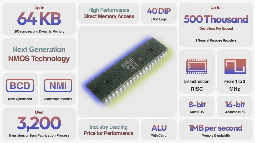
Marketing the MOS 6502 as a Next-Gen Processor
Why is this TechHistory meme funny?
Level 1: Small Chip, Huge Deal
Imagine you have a really old toy that your grandparent loved as a kid. Back then, it was the coolest thing ever, even if by today’s standards it’s super simple. This meme is like saying: “Wow, in the 1970s, a computer chip with just a few thousand tiny switches and an 8-bit brain was like a superhero!” It’s funny because today our gadgets have millions of those tiny electronic “switches” (called transistors) and are millions of times more powerful – yet we hardly think about it. It’s like someone bragging that their old TV had 8 channels (which was awesome in the past), while now we stream endless shows on a flat-screen TV and 8 channels sounds adorably quaint. The meme shows a pretend advertisement for that old 8-bit computer chip, proudly listing its abilities in rainbow colors. The joke is that what used to be bragging rights – things like “can handle 64KB of memory!” or “runs at 1 MHz!” – now feel tiny and cute. It’s as if a car from 1910 boasted “goes 30 miles per hour!” and we smile because modern cars go much faster. So, the meme makes us chuckle and feel a bit warm inside, realizing how far technology has come. It’s showing that in the early days of computers, even a small chip was a huge deal, and remembering that just makes us appreciate today’s tech wonders even more.
Level 2: Decoding the Datasheet
Let’s break down the retro specs shown in this meme and explain what each means in real-world terms. These were once top-of-the-line features for an 8-bit microprocessor like the 6502:
“Up to 64 KB – 200 nanosecond Dynamic Memory” – The 6502 could address up to 64 KB of RAM directly because it had a 16-bit address bus (2^16 addresses = 65,536 bytes). In the late 1970s, 64 KB was a large memory space for a microcomputer. The mention of “200 nanosecond” dynamic memory refers to the typical speed of DRAM (dynamic RAM) chips then – 200 ns access time. This means the memory could be read/written in about 0.2 microseconds. Since a 1 MHz CPU has a cycle of 1000 ns, a 200 ns memory was plenty fast to keep up. Dynamic memory needs periodic refreshing (because bits are stored as charge on tiny capacitors), but it was the common way to get higher density RAM. So essentially, they’re bragging that the CPU can work with a healthy amount of memory (tens of kilobytes!) at respectable speeds for the time.
“High Performance Direct Memory Access” – Direct Memory Access (DMA) is a feature/technique that allows peripherals (like disk controllers, graphics chips, etc.) to transfer data to or from RAM without the CPU handling each byte. In a system with the 6502, an external DMA controller or another chip could briefly take control of the buses to move data faster or do it while the CPU is doing other things. The phrase “High Performance DMA” is a bit of marketing fluff here – the 6502 itself didn’t include a built-in DMA engine (like some modern processors do). But it did have provisions to facilitate DMA: for example, the 6502’s READY (
RDY) pin could pause the CPU, and the bus could be tri-stated to let another device transfer data. In practice, systems like the Commodore 64 took advantage of this: the video chip could perform memory fetches for graphics while halting the 6502 briefly. So this statement means the chip is designed to cooperate with DMA for better overall performance in a system.“40 DIP – 5 Volt Logic” – This describes the physical package and electrical requirements. 40 DIP means a 40-pin Dual In-line Package, which is the classic rectangular black chip with two rows of 20 metal pins (legs) on each side. The 6502 came in such a package, making it easy to plug into sockets or solder onto boards. 5 Volt logic means it uses a single +5V power supply and its signals are 0 V for logic “0” and 5 V for logic “1” (compatible with TTL logic levels of that era). Back then, +5V was the standard for digital ICs. This spec point basically tells you it’s a typical chip that fits into the existing electronics ecosystem (needs a 5V supply, works with other 5V components, and you’ll need to allocate 40 pins for it on your circuit board). Today, most modern microprocessors use lower voltages (3.3V, 1.8V, or even down to ~1V for cores) and come in very different packages (like BGA – Ball Grid Array – with hundreds of tiny solder balls instead of big pins).
“Up to 500 Thousand Operations Per Second – 3 General Purpose Registers” – This is highlighting performance and the CPU’s internal registers. 500 thousand operations per second is roughly the number of instructions the 6502 could execute at its top speed. At 1 MHz clock, if each instruction took an average of ~2 cycles, that’s ~0.5 million instructions per second. If clocked at 2 MHz, it could approach 1 million ops/sec. They say “up to” because it depends on clock speed and the mix of instructions. Compared to modern processors (which do billions of operations per second), this is a tiny number, but at the time it meant the chip could do a lot of work for its cost. The 3 general-purpose registers refer to the CPU’s primary programmer-visible registers: the Accumulator (A), and two index registers (X and Y). These are like small scratchpad variables inside the CPU that hold data for calculations and addressing. Having only 3 main registers means the CPU design is simple, but also means the programmer often has to use memory (stack or zero-page RAM) to store extra variables because there aren’t many registers. Many other CPUs of the time (like the Intel 8080 or Zilog Z80) had more registers, but the 6502 made do with fewer to keep the transistor count low and instruction set lean.
“Next Generation NMOS Technology” – NMOS stands for N-type Metal-Oxide-Semiconductor, a transistor technology used to build the chip. This tells us the 6502 was built using NMOS transistors. “Next Generation” in this context likely implies it was using a then-modern fabrication process and transistor design that improved speed or cost over previous chips (earlier CPUs like the Intel 4004/8008 or some peripherals were made in PMOS or in larger geometry processes). NMOS-only logic was faster than PMOS logic because NMOS transistors could switch faster when pulling signals down to 0. However, NMOS logic typically uses pull-up resistors or active loads, resulting in higher power draw especially when static. Despite that, NMOS was state-of-the-art in the mid-70s for performance. It wasn’t until the 1980s that CMOS (which uses complementary pairs of transistors, N and P, to greatly reduce power consumption) became mainstream for CPUs. So this spec is basically saying: our chip uses the latest transistor tech for great speed.
“BCD – Math Operations” – BCD stands for Binary Coded Decimal. This feature means the 6502’s arithmetic logic unit can directly support decimal arithmetic. In BCD mode, each byte isn’t interpreted as 0–255 binary, but as two decimal digits (0–99, with 4 bits for each digit 0–9). The 6502 had a flag (the
Dflag in its status register) that, when set, caused its addition and subtraction instructions (ADCandSBC) to perform decimal adjusts. Essentially, after a normal binary addition, the ALU would adjust the result so that the lower 4-bit nibble stays within 0–9, and similarly adjust the higher nibble if needed (taking the carry into account). Why is this useful? Because if you want to do monetary calculations or work in human-readable decimal in assembly, BCD saves you from writing extra code to correct the results – the hardware handles it. In the context of a 1970s spec sheet, “BCD Math Operations” was noteworthy because not all CPUs had this. It hinted that the 6502 could easily be used in business and calculator-like applications. For example, if you were writing a financial program or a calculator firmware, native BCD support would make it simpler. It’s a bit of a niche feature today (high-level languages handle decimal math in software or via libraries, and modern CPUs don’t bother with BCD in hardware), but in the 6502’s time, it was a practical selling point.“NMI – 2 Interrupt Priorities” – This refers to the interrupt system of the CPU. Interrupts are signals that can pause the normal program flow and jump to a special routine (an interrupt handler). They’re crucial for responding to asynchronous events (like input from a user, timers, or hardware signals). The 6502 supported two kinds of interrupts: a regular IRQ (Interrupt Request) which is maskable (the program can disable it temporarily), and an NMI (Non-Maskable Interrupt) which cannot be disabled by normal program instructions – it will always get through (except maybe if another NMI is being processed). Because the NMI can’t be masked off, it’s considered a higher priority interrupt than the regular IRQ. So effectively, there are two priority levels: NMI (high priority, urgent, often used for things that must be handled like device failure signals or vertical blank interrupts in video hardware), and IRQ (lower priority, can be postponed if needed). When the meme says “2 Interrupt Priorities”, it’s highlighting that the 6502 can distinguish an NMI from a normal IRQ and handle them separately. Many early microprocessors did have an NMI line (for example, the Z80 and 8080 had similar concepts), but again, the datasheet-style callout is bragging: we have a dedicated non-maskable interrupt line for critical events! For a programmer, this meant more control: you could ensure some critical event (like a clock tick or emergency stop) would always get serviced, even if you had disabled normal interrupts temporarily.
“Over 3,200 Transistors on 8 µm Fabrication Process” – This is the proud declaration of the chip’s complexity and manufacturing tech. 3,200 transistors is literally the count of active transistor devices on the CPU. Each transistor is like a tiny electronic switch, and together they form all the logic gates, flip-flops (storage bits), and drivers in the processor. Today’s chips have transistors in the billions, so 3,200 sounds minuscule, but at the time it was on par or slightly less than its competitors (the Intel 8080 had around 4,500 transistors; the Motorola 6800 had about 4,100). The 6502 was efficient in design – achieving similar or better computing capability with fewer transistors, which was one reason it could be sold cheaper. The 8 µm process indicates the process node used in manufacturing. 8 µm (micrometers) is 8 millionths of a meter. This figure is roughly the size of the smallest features (like the transistor gate length) on the chip. By comparison, modern CPUs are made with processes like 5 nm (nanometers) or 7 nm – that’s 0.005 µm or 0.007 µm feature sizes, extremely smaller. The process size and transistor count together tell us how advanced the chip was in 1975: 8 µm was a leading-edge process for that era (the earlier Intel 4004 in 1971 used ~10 µm, so by mid-70s 8 µm was aggressive). A smaller process allows more transistors in the same chip area and usually higher speeds (shorter distances for signals to travel). So this line basically screams: we used a modern fabrication technique to pack in an unprecedented 3,200+ transistors on one chip. It was indeed a bragging point – getting thousands of transistors to work together reliably was non-trivial at the time. HardwareEvolution at work!
“Industry Leading Price for Performance” – This is more of a marketing slogan than a spec. It means that, for the amount of performance the 6502 offers, its cost was exceptionally low compared to others. As mentioned, the 6502 was introduced at a fraction of the cost of similar CPUs, which made waves in the industry. So “price for performance” is basically value: how much bang (computing power) you get for your buck. The 6502 led the industry in this metric, meaning no competitor could match how cheaply you could get this level of computing. For an engineer or company choosing a CPU in 1975-1977, this was huge. It meant you could build your product (be it a hobby kit computer, a video game console, etc.) much cheaper. This drove its adoption in many famous systems. So, this point on the meme is winking at that legendary affordability. In a tongue-in-cheek way, it’s like those car commercials saying “best fuel efficiency in its class!” – here it was best compute-per-dollar in its class.
“ALU With Carry” – The ALU is the Arithmetic Logic Unit, the part of the CPU that does calculations (like addition, subtraction, bitwise operations, etc.). “With Carry” refers to the carry flag mechanism. When you add two numbers and the result exceeds the maximum value that can be held (for 8 bits, that’s 255 max), you get a carry-out to the next higher bit (like in addition: 9 + 5 = 14, we write 4 and carry 1 to the next digit). The 6502’s ALU had a carry flag in its status register to hold that extra bit, so it could be used for multi-byte arithmetic. For example, to add two 16-bit numbers, the CPU adds the low bytes, sets or clears the carry, then adds the high bytes along with that carry. This is standard for basically all CPUs – you need a carry to do proper multi-word math and to detect overflow conditions. So why highlight it? In the context of a flashy datasheet, it might sound like a given, but possibly not all microcontrollers supported easy use of the carry for multi-byte BCD operations, etc. The 6502’s instructions (
ADCandSBC) explicitly use the carry both as input and output (you have to manage the carry flag when doing sequence of additions or subtractions). The marketing blurb “ALU With Carry” assures that yes, the chip has a full-featured ALU that can handle carry/borrow – which implies it’s capable of doing arithmetic on numbers larger than 8 bits via software routines. Essentially it’s saying the chip isn’t crippled in the math department; it can perform the standard operations expected of an 8-bit CPU (again, it’s kind of a funny thing to boast about, but they wanted to list everything that could set them apart).“56 Instruction RISC” – This bullet point is a playful one, blending eras. The MOS 6502’s instruction set (the list of operation codes it understands) can be counted in different ways, but it’s often said to have 56 mnemonic instructions (not counting all the different addressing modes separately). If you count every addressing mode variation as a separate opcode, the 6502 actually has 151 opcodes (with a few unused holes). But listing it as “56 Instruction” likely counts the unique operations (like LDA, STA, ADD, SUB, JMP, etc.). Calling it RISC (Reduced Instruction Set Computer) is a bit anachronistic here – RISC was a design philosophy that emerged in the 1980s (notably with processors like the MIPS and ARM architectures), emphasizing a small set of simple instructions for efficiency. The 6502 wasn’t designed as a RISC per se, but it did have a relatively small, efficient core instruction set out of necessity. By modern standards, the 6502’s instructions are simple and few enough that one could whimsically label it RISC-like. The meme is having fun by mixing terminology: in the ’70s a 56-instruction set was just “the instruction set”, nothing special named, but someone reading it today with knowledge of later tech might chuckle, “Ha, 56 instructions, that is quite reduced indeed!” In practical terms, this spec means the chip had all the essential operations needed but kept the instruction count low (which simplifies design and can improve speed, since the decoder is simpler). The 6502 could do loads/stores, arithmetic (add/sub), bit operations, control flow (jumps, branches), etc. Even though it had fewer instructions than some rivals, it was not at a disadvantage – in fact, it often executed things faster and more efficiently because each instruction was small and quick. So, “56 Instruction RISC” conveys: we have a lean, mean instruction set that gets the job done without unnecessary complexity.
“From 1 to 3 MHz” – This refers to the clock speed range of the processor. The base MOS 6502 ran typically at 1 MHz in many systems (like the Apple II and earliest Commodore PETs). Later, depending on the manufacturing process and the specific variant, some could run at 2 MHz or even a bit beyond. In fact, the 6502’s successor or CMOS versions (like the 65C02) could run at 4 MHz or more, and some systems (like the BBC Micro’s 6502) ran around 2 MHz. The “up to 3 MHz” likely refers to the highest official clock rate of certain versions (like the 6502A or 6502B). Essentially, it’s telling you the chip is flexible and can be used in systems with different speed requirements – it’s stable across this range. Nowadays, 1-3 MHz is extremely slow (modern CPUs are around 3,000 MHz, i.e., 3 GHz, and even microcontrollers often run at tens or hundreds of MHz), but at the time, 1 MHz was a common baseline for microprocessors. If you could push to 2 or 3 MHz, you had a speed demon on your hands! Each MHz increment was significant because it scaled the execution speed linearly. So advertising a top-end of 3 MHz says the design has headroom and is not limited to just the initial 1 MHz. It’s akin to how modern CPUs might advertise turbo speeds (like “up to 5.0 GHz on demand”). It gave engineers confidence that the chip could be used in more performance-critical roles if needed, or that future versions would scale up in speed.
**“8-bit Data BUS” & “16-bit Address BUS” – These are fundamental descriptors of the CPU’s architecture. 8-bit data bus means the CPU processes data in 8-bit chunks. The internal registers like A, X, Y are 8 bits wide, and the arithmetic operations it does (add, subtract, etc.) are on 8-bit values (0 to 255). If you have bigger numbers, the CPU has to handle them in pieces (multiple operations and using the carry, as mentioned). An 8-bit data bus also means when it reads or writes memory, it moves one byte at a time on an 8-line bus. 16-bit address bus means the CPU can address memory locations using 16-bit addresses (0 to 65535 in decimal). Each address corresponds to one byte in memory, so that gives the 64 KB addressable range. Together, “8-bit CPU” and “16-bit address bus” roughly define the 6502 as an 8-bit microprocessor (8-bit usually refers to the data width). Many microcomputers of that era were “8-bit”, whereas later ones (like the 8086 or Motorola 68000) were “16-bit” or more. This particular combination (8-bit data, 16-bit address) was sweet-spot for cost and capability for a long time in small systems. For a newcomer: think of it like the width of a highway (8-bit data bus is like 8 lanes for data traffic, fairly narrow by today’s standards) and the range of addresses as the number of houses it can visit (16-bit addresses means it can directly visit 65,536 houses in memory-town). More bits in data or address would mean exponentially more capacity and complexity, which at the time wasn’t feasible in a low-cost product. So those specs tell you the scale of data it deals with and how much memory it can use.
“1 MB per second Memory Bandwidth” – This ties into the clock speed and bus width. If the CPU is running at 1 MHz and it can fetch 1 byte each cycle from memory (which, roughly, the 6502 does – it performs a memory fetch almost every cycle for instructions or data), then it can read 1,000,000 bytes per second, which is about ~1 MB/s (where MB here is likely in the decimal sense for simplicity). In reality, memory bandwidth depends on how the CPU accesses memory, and some cycles might be idle or used for internal operations, but marketing-wise, you’d say “up to 1 megabyte per second”. If you clock it at 2 MHz, that becomes 2 MB/s, etc. So it’s giving a sense of how fast data can move between the CPU and memory. Today, memory bandwidth is quoted in much larger terms (e.g., 25.6 GB/s for a dual-channel DDR4 3200 MT/s system). So 1 MB/s is tiny, but in the late 70s, being able to move a million bytes in a second with a single cheap chip was fantastic. For perspective, loading an entire 64 KB memory could be done in about 1/16th of a second at 1 MB/s – not bad for that era. It meant if you had a cassette tape or floppy disk loading data into memory, the CPU/memory system could handle it (I/O devices like disks or tapes were much slower anyway). So the bottleneck wasn’t the memory bus for typical use, which is a good thing and was worth pointing out to system designers.
In summary, each of these specs and buzzwords was highlighting an important aspect of the 6502’s capabilities or design: how much memory it can use, how fast it is, how it handles math and interrupts, what technology it’s built from, etc. In the context of the meme, they’re presented with a bit of tongue-in-cheek flair – each spec that once would have been an engineer’s pride now looks almost cute. But understanding them gives you an appreciation for what this little retro microprocessor could do and why it was such a big deal in computing history.
Level 3: 8-bit Glory Days
This meme beautifully captures the nostalgic humor of TechHistory by parodying a vintage marketing specsheet for the classic 6502 CPU. The image is styled like a 1970s datasheet or magazine ad, complete with optimistic slogans and rainbow-gradient text proudly proclaiming features: “Next Generation NMOS Technology!”, “High Performance Direct Memory Access”, “Industry Leading Price for Performance”. For anyone who’s been around hardware long enough (or thumbed through old computing magazines), these phrases hit home. They echo the genuine advertisements and datasheets of the late 70s and early 80s, when every byte and every Hertz was a big deal and marketers weren’t shy about bombastic claims. Senior engineers or retro computing enthusiasts can’t help but grin at this, because it reads like a time capsule from the 8-bit Glory Days – a time when 3,200 transistors on a chip truly gave you bragging rights and an 8-bit Data BUS was enough to launch a revolution in home computing.
The humor here comes from the stark contrast between then and now. The meme lists specs like a greatest-hits album of the 6502’s capabilities, all of which sound absurdly humble by today’s standards. “Up to 64 KB of memory!” — that’s a laughably tiny amount of RAM today (your phone probably has 4 GB or more, which is about 65,000 times larger), but back when LegacyHardware like the 6502 reigned, 64 KB was generous (many early machines had far less). “Up to 500 Thousand Operations Per Second” – modern CPUs execute billions of operations per second, so half a million sounds like nothing, but on a 1 MHz chip each instruction counted, and hitting ~0.5 MIPS was enabling all kinds of new software. By framing these specs as boastful bullet points, the meme is winking at those in the know: Remember when this was cutting-edge? It triggers a kind of camaraderie among experienced developers and hardware folks — we collectively remember or imagine how excited engineers must have been to achieve these milestones. It also underscores just how fast hardware evolves. The title line “When 3,200 transistors were serious bragging rights for an 8-bit CPU” says it all: nowadays we talk about multi-core processors with millions of transistors each dedicated to caches or graphics units, but around 1975, hitting the 1,000+ transistor scale for an affordable CPU was like landing on the moon.
A senior perspective also picks up on the optimistic tone of the spec sheet parody. In the ’70s, microprocessor companies were in a race, and the marketing often had a gee-whiz enthusiasm. The meme’s pastel color blocks and bold fonts screaming things like “BCD – Math Operations” and “ALU With Carry” mimic that era’s style — as if each of those features were revolutionary breakthroughs (and at the time, they kind of were!). For instance, including a decimal math mode (BCD) in the instruction set was a selling point because it meant the chip could easily handle currency or calculator-like tasks. The presence of an NMI (Non-Maskable Interrupt) line gave system designers a way to handle urgent signals (like a power failure notice or an emergency stop in an industrial machine) reliably — a notable improvement in robustness for embedded applications. And “Direct Memory Access” support signified that this CPU could play nice in more complex systems where DMA controllers might take over the bus; that’s something we assume as standard now, but then it made the 6502 suitable for more demanding tasks like disk I/O or video rendering in games.
Reading these spec call-outs, veteran developers might recall the classic devices powered by the 6502 and its variants: the Apple II, the Commodore 64, the Nintendo Entertainment System (which used a 6502 derivative). Those were seminal products in the history of personal computing and gaming, and they all ran on this humble 8-bit core. So there’s an undercurrent of respect amid the humor: this little chip with 3,200 transistors had an outsized impact. It taught an entire generation of programmers the art of EmbeddedSystems and low-level hacking. Many senior folks fondly remember writing assembly code on 6502-based machines, where you manipulated bytes directly, used those three registers creatively, and maybe even toggled that BCD mode or handled NMIs for game controllers. The meme’s comedic exaggeration (“56 Instruction RISC” – cheekily labeling the 6502’s modest instruction set as if it were a trendy modern RISC architecture) also pokes fun at how terminology evolves. In the 1970s nobody called the 6502 RISC; that buzzword came later. But from today’s vantage point, its instruction set does look pretty “reduced” compared to the sprawling complex instruction sets of later CISC processors. It’s a bit like saying “Our old jalopy was basically an electric car – it didn’t go fast and had no frills, which is how modern efficient cars are!” – a humorous retroactive re-branding.
Another layer of humor is the “Industry Leading Price for Performance” blurb. That is a very marketing phrase, and historically, it’s spot-on: the 6502 was dirt cheap for what it delivered, which is one big reason it proliferated. Seeing that phrase in a meme context makes experienced readers chuckle because it’s such a HardwareHumor cliché now – every new chip or gadget today claims “best performance per dollar” or “unmatched value”, often with some asterisk. But in the 6502’s case, it really did shake up the industry by making computing affordable (it helped spawn a whole ecosystem of home computers and consoles). Senior engineers might even recall famous anecdotes, like at the Wescon trade show in 1975 where MOS Technology shocked attendees by selling the 6502 for $25, undercutting everyone – truly a “hold my beer” moment in Hardware history. That spirit of scrappy innovation is part of the legend this meme is tapping into.
In essence, the meme’s joke is a big “Look how far we’ve come!” The once-mighty specs of a revolutionary retro_microprocessor now read like quaint, adorable footnotes. It’s not mocking the 6502 out of malice – it’s more of a warm, proud chuckle. Think of a veteran athlete looking at footage from their prime, amazed at how the game has changed. Seasoned devs have a bit of that proud-yet-amused feeling: HardwareEvolution has run laps around what was imaginable in the 70s, and yet we salute those early achievements because without them, we wouldn’t be here. The image’s parody datasheet format really drives home that feeling. Each spec in its rounded box with colorful text is almost like a panel in a comic strip, each delivering a punchline by mere context: “40 DIP – 5 Volt Logic” (hey, remember when 5V was standard and chips came in big dual-inline packages you could actually see and solder by hand? Today’s chips are BGA blobs you need a microscope to debug!). “From 1 to 3 MHz” (amazing range! – today our CPUs scale from like 1 to 4 GHz with dynamic frequency scaling and still we demand more). Even “ALU With Carry” – that one always gets a chuckle because of course the ALU has a carry flag; it’s such a basic CPU concept that highlighting it feels silly, but for marketing, any spec that could be an advantage was spotlighted. It’s akin to a car brochure proudly stating “Comes with a steering wheel!” – obvious now, but if others at the time lacked it or did it differently, you’d boast about it.
Senior devs also appreciate the undercurrent of how low-level programming was in those days. The 6502 gave you a simple, raw interface to the machine. No abstractions – you directly manipulated memory addresses (hence the 16-bit address bus mention), toggled flags, and counted clock cycles. The meme brings that to mind implicitly. There’s a bit of shared war-story humor: “I remember trying to squeeze code into 2 KB because the system had only 4 KB free after the screen buffer, or using every trick because the CPU ran at 1 MHz and we needed smooth animation.” Modern devs fret if their web app takes 200 MB of RAM; a 6502 dev had 0.0002 GB to work with! That perspective is both humbling and amusing. So when we see these old specs dressed up with marketing glitz, the experienced among us smile and think, “Yes, those were the specs and we actually did incredible things with them. Hard to believe, isn’t it?”
Finally, the meme might spark recognition about how even today’s simplest gadgets owe a debt to those days. A lot of EmbeddedSystemsAndIoT devices today (simple sensors, hobbyist microcontrollers like Arduino) have specs not far off from the 6502 era. An Arduino Uno’s MCU, for example, has an 8-bit CPU at 16 MHz, 32 KB of flash, 2 KB of RAM – not too dissimilar in scale, and also running on 5V logic for many variants. So in a funny way, this “old” spec sheet could almost describe a modern microcontroller’s ballpark, yet we’d never boast about those numbers now for a general-purpose computer. It’s only acceptable for tiny embedded use-cases. This highlights how expectations have shifted. What was “general purpose” computing (running BASIC interpreters, games, word processors on a 6502 machine) is now ultra-embedded territory — the realm of blinking LEDs and reading sensors. Meanwhile, “general purpose” today means running a full multitasking OS with gigabytes of memory. That dramatic shift in baseline is the heart of the meme’s humor: yesterday’s superstars are today’s featherweights. It’s a healthy reminder of progress and also an affectionate nod to the giants on whose small shoulders we stand. In short, “8-bit Glory Days” were real, and this meme captures their spirit with a hearty wink.
Level 4: Architecture Archaeology
Back in the mid-1970s, the MOS 6502 microprocessor was at the cutting edge of HardwareEvolution – a true artifact of early LowLevelProgramming lore. With just over 3,200 transistors etched in silicon on an 8 µm (micrometer) process, it was a marvel of minimalist design. To put that in perspective, modern CPUs pack billions of transistors on chips fabricated with features only dozens of nanometers wide (an 8 µm transistor is about 1600 times larger than a 5 nm transistor!). Such drastic scaling over decades is a testament to Moore’s Law, the observation that transistor counts double roughly every two years. In 1975, each transistor was precious – they had to implement an entire CPU with a budget of a few thousand switches. This led to an elegantly simple architecture: only 3 general-purpose registers (Accumulator A, index registers X and Y), no on-chip cache, and a lean control logic with no microcode ROM. The designers used NMOS technology, meaning the chip’s logic was built from N-channel MOSFETs. NMOS was faster than the earlier PMOS tech (which powered earlier chips like the Intel 4004), but it drew static current (through resistive loads or depletion transistors), making it hot and power-hungry by today’s standards. Each transistor on the 6502 had to pull its weight – they even included hardware support for BCD (Binary Coded Decimal) arithmetic, which required extra logic to adjust sums for decimal digit values. Supporting BCD was important at the time for business calculations (e.g. currency) because high-level software libraries weren’t commonplace – hardware had to step up for functionalities we now take for granted in software.
The 6502’s instruction set architecture is often described as somewhat RISC-like (Reduced Instruction Set Computer) in hindsight, since it had a relatively small core of ~56 instructions and favored simple operations. However, true RISC design principles (like fixed instruction lengths, load/store architecture, deep pipelining) were only formalized in the early 1980s. The 6502 didn’t have a pipeline with hazard detection or fancy branch prediction – at this scale, each instruction was executed in a straightforward sequence (though internally it did overlap instruction fetch and execution to improve throughput). There were no dedicated hardware multiply/divide units, no out-of-order execution, and certainly no speculation: the entire chip’s transistor count wouldn’t even register as a rounding error in a modern core’s control unit. Yet this little 8-bit CPU could be clocked up to 1 MHz (and later variants to 2 or even 3 MHz), meaning a clock period of 1 microsecond. The mention of “200 nanosecond Dynamic Memory” in the datasheet highlights memory access time – around 0.2 µs for a RAM access, which was considered high-speed memory that could keep up with a 1 MHz clock (since one CPU cycle was 1000 ns). There was no on-die memory management unit or caches, so memory was accessed directly over the external bus; hence, bragging about ~1 MB/s memory bandwidth (1 byte per microsecond) made sense. For comparison, today’s DDR4 RAM can transfer on the order of 20 GB/s (over 20 billion bytes per second) to a CPU – a different universe of performance.
It’s fascinating from a TechHistory perspective how the 6502’s tiny transistor count constrained and shaped its capabilities. The 16-bit address bus limited it to 64 KB of addressable memory space. This wasn’t seen as a severe limitation initially – 64 KB was actually huge for microcomputers of that era (the famous Apple II shipped with 4 KB or 16 KB of RAM in early models, expandable up to that 64 KB ceiling). Designers and programmers accepted such limits and wrote incredibly efficient code to work within them. The EmbeddedSystems of the late 70s and early 80s – home computers, game consoles, toy robots – thrived with these constraints. In those systems, the 6502 often ran the show alongside a few support chips (like the VIA 6522 I/O chip, or graphics/audio co-processors in consoles). It even allowed Direct Memory Access by external devices: the 6502 had a RDY pin and could relinquish the bus on demand, so peripheral chips (like the legendary Commodore 64’s VIC-II graphics chip or DMA controllers in later systems) could transfer data while the CPU idled for a few cycles. This was a rudimentary form of DMA, nothing like the integrated DMA engines of modern SoCs, but it was enough to tout “High Performance Direct Memory Access” in marketing – it meant a clever system designer could have smooth graphics or disk I/O without bogging down the CPU.
From a hardware architecture viewpoint, the 6502 was delightfully simple, but that simplicity was its strength. Fewer transistors meant a smaller chip die, which in turn meant higher yield per silicon wafer and lower cost. In fact, the Industry Leading Price for Performance was no empty boast – the chip famously debuted at around $25, dramatically undercutting competitors like the Motorola 6800 (which cost around $175 initially) and Intel 8080. This aggressive pricing (made possible by the 6502’s minimal transistor design and some savvy business) catalyzed its widespread adoption. The 6502 didn’t need fancy superscalar execution or millions of gates of cache coherence logic; it could handily execute about 0.5 MIPS (Million Instructions Per Second) at 1 MHz, since many instructions executed in 2 cycles or more. Half a million operations per second for a ~$25 chip in 1975 was revolutionary – it put computing power in the hands of hobbyists and helped ignite the personal computer revolution. Consider that today we measure CPU speeds in GHz (1 GHz = 1,000 MHz) and performance in tens of billions of operations per second; the old 6502’s specs seem quaint, but they laid the groundwork for everything to come. Modern high-performance processors devote enormous transistor budgets to features like pipelines, branch predictors, and multi-level caches to push clock speeds beyond 3 GHz and IPC (instructions per cycle) to superscalar heights. The 6502 had none of those luxuries – it was a lean, blocking CPU: one instruction at a time, crunching away with its tiny 8-bit ALU (which did handle a Carry flag for multi-byte arithmetic, crucial for adding numbers larger than 255). This forces us to appreciate how ingeniously the engineers of the day solved problems under severe resource constraints. They engaged in a form of architecture archaeology – digging through logic optimizations to save every transistor, multi-purposing circuits, and using clever tricks like zero-page memory (the first 256 bytes of memory acted almost like fast registers for the 6502 due to special addressing modes) to maximize performance. It’s a stark contrast to today’s sprawling silicon giants: for instance, a modern 8-core desktop CPU might have on the order of 10^9 transistors and an entire team of logic designers for each subsystem. The entire 6502 design, with just a handful of engineers, could fit in the corner of one of those modern cores. In fact, amusingly, the transistor_count_3200 of a 6502 is so low that you can simulate it in software extremely efficiently, or even rebuild it on an FPGA using only a tiny fraction of the FPGA’s resources. Enthusiasts have etched 6502 replicas on modern processes as a hobby, and you could literally have a complete 6502 core occupying only a sliver of silicon on a contemporary chip (some modern microcontrollers include small 8-bit cores as peripherals – the legacy of the 6502’s era lives on in spirit).
At this granular level, the meme highlights a microcosm of Hardware progress. Each spec that was brag-worthy in the 1970s ties to fundamental computer architecture concepts. It’s both educational and humorous to contrast them with today’s reality. The eight-bit data bus and 16-bit address bus reflect fundamental design choices that simplified chip complexity but limited data width and memory range. The lack of pipelining or caches meant the CPU’s performance scaled almost linearly with clock speed and instruction count – so listing “Up to 3 MHz” and “500 Thousand Operations Per Second” was straightforward and honest (no turbo boost, no hyperthreading, just raw cycles and instructions). The pride in “BCD math” and having an ALU with carry shows how even small features (like decimal mode for arithmetic or proper carry propagation) were selling points when every additional capability was hard-won in silicon. And boasting about an NMI (Non-Maskable Interrupt) line for “2 Interrupt Priorities” underscores how early CPUs were learning to handle external events – a precursor to the sophisticated interrupt controllers and multi-core interrupts we have now. These design elements are part of the legacy hardware DNA that modern systems inherited and expanded upon. The meme effectively serves as an archaeological dig into the strata of computing history: each bullet point around that image is like a fossil of past innovations, and understanding them requires digging into why they mattered in their time. It reminds seasoned engineers of how EmbeddedSystemsAndIoT were born — from tiny chips like this — and gives context to newbies about why older programmers sometimes wax poetic about “only 64 KB of RAM and we were happy!”. In essence, we’re looking at a retro microprocessor highlight reel: a greatest-hits of 1970s silicon bragging rights, presented with tongue-in-cheek reverence for how far we’ve come.
Description
This image is a satirical infographic presenting the specifications of the vintage MOS Technology 6502 microprocessor as if it were a modern, cutting-edge product. The layout is clean and contemporary, with a central image of the 40-pin DIP chip surrounded by callout boxes with smooth gradients. These boxes highlight its technical specs, including: 'Up to 64 KB' of memory, 'Up to 500 Thousand Operations Per Second', 'Next Generation NMOS Technology', 'Over 3,200 Transistors on 8µm Fabrication Process', an '8-bit Data BUS', '16-bit Address BUS', and a clock speed of 'From 1 to 3 MHz'. The humor is derived from the stark contrast between the modern, hyperbolic marketing language ('High Performance', 'Industry Leading') and the extremely modest capabilities of this 1970s-era chip. For experienced engineers, this is a nostalgic nod to a processor that powered iconic machines like the Apple II and Commodore 64, while also poking fun at how dramatically the scale of computing has changed due to Moore's Law
Comments
22Comment deleted
The 16-bit address bus was a brilliant feature, ensuring developers would never be tempted by the decadent excess of addressing more than 64KB of RAM
Remember when "high-performance DMA" meant a whole megabyte per second? These days our CI pipeline logs hit that before the coffee in Jenkins finishes brewing
Love how they're marketing 3 registers like it's a feature - modern devs complain when they only have 32. Next they'll be bragging about the revolutionary 'single accumulator architecture' and 'industry-disrupting 256-byte stack limitation'
Ah yes, the golden age when '64 KB ought to be enough for anybody' was actually aspirational, not a misquote. This chip's 500,000 operations per second would struggle to render a single frame of a modern loading spinner, yet somehow we managed to land on the moon with less. Today's developers complaining about memory constraints while their Electron app consumes 2GB of RAM should spend a day with these 3 general-purpose registers and 1MB/s memory bandwidth - suddenly that O(n²) algorithm doesn't seem so bad when your entire address space fits in a modern CPU's L2 cache
8088's 66 instructions ran the PC era; today's VMs need 66GB just to enumerate theirs
56 instructions, three registers, and 1-3 MHz, yet it still boots faster than our SPA behind a service mesh, API gateway, and six JSON parsers
56‑instruction “RISC”, 64KB, and three registers - the stack where zero page is your cache, and the end‑to‑end throughput still beats our JSON microservice once you factor serialization and egress
bot Comment deleted
No no, that chip generally changed my life for real I am now motivated enough to build a PC Comment deleted
But Julia is still a spam bot :) Comment deleted
That was supposed to be the joke since I don't really think anyone would be inspired by a 64kb processor Comment deleted
Depends on when it happened… ;) Comment deleted
True... One might need only this bit of information to invent a world changing device Comment deleted
Intel 8080 was very inspiring. Comment deleted
I followed Ben Eater's videos about the 6502, it's an incredible series, and an incredible piece of technology Comment deleted
Yeah, but can it run DOOM? Comment deleted
Cool. And it is enough for a lot of good apps Comment deleted
Z80 the best. No 64 KB limit. Comment deleted
Imagine putting 4gb in it Comment deleted
Actually there is. z80 can only address 64 kilobytes at a time. More memory is achieved by dividing memory into pages and switching between these pages in a window. this is used by both the ZX Spectrum with z80 architecture and the NES with 6502 architecture, and by many other systems too. Comment deleted
What a funky looking centipede. Comment deleted
Are those actually specs of the new iPhone? Doesn't matter I will buy it because its apple. (Dw only apple thing I have is iPhone 8 and unless its free I wont upgrade) Comment deleted