Skip to content
DevMeme
1657 of 7435
The Great Wave of Circuitry
Hardware Post #1853, on Aug 5, 2020 in TG

The Great Wave of Circuitry

Why is this Hardware meme funny?

Level 1: Fancy Wires

This is funny because it looks like someone made a famous ocean wave out of tiny electronic roads. It is like drawing a beautiful picture using only train tracks and traffic lines. Engineers laugh because those little lines are usually serious work, but here they have been arranged into something dramatic and pretty. The feeling is: "I was supposed to build a machine, but somehow I made art."

Level 2: Traces Make Waves

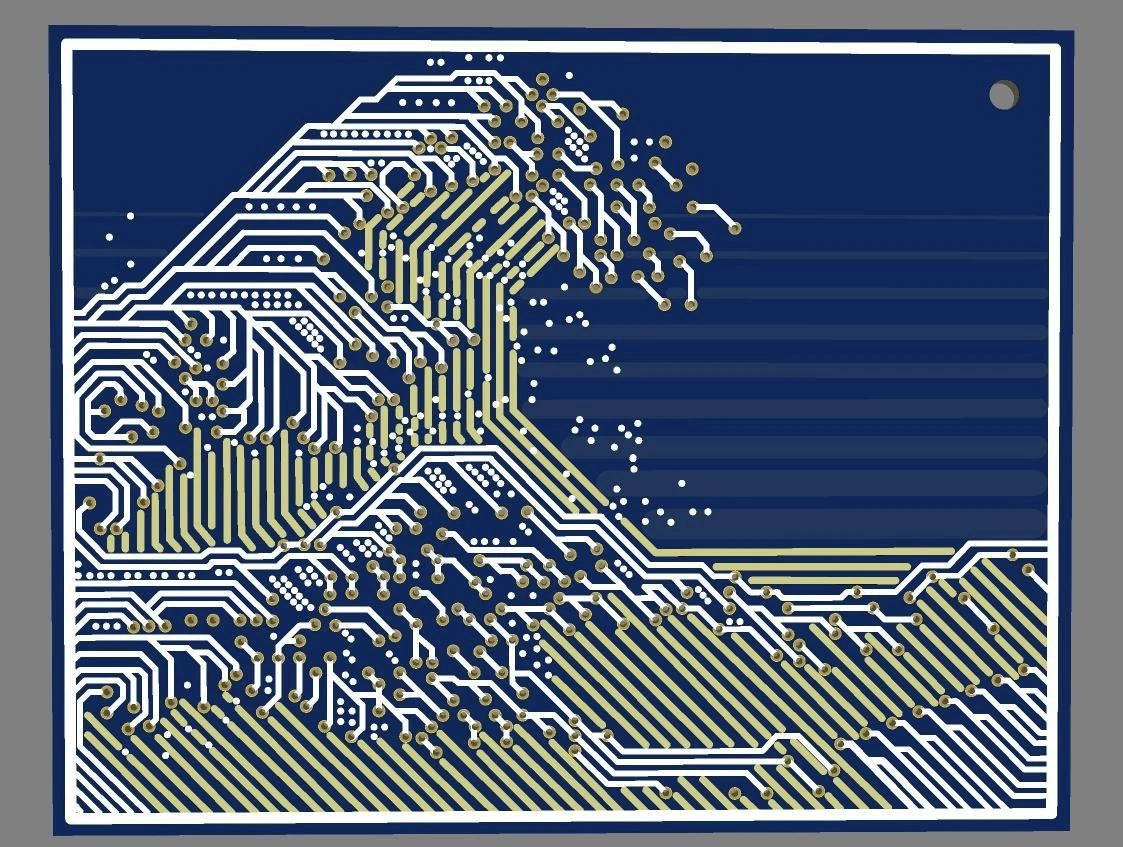
A PCB, or printed circuit board, is the flat board that connects electronic components. The long white and gold lines in the image are traces, which are copper pathways that carry electrical signals or power. The many small dots are likely vias and pads. A via lets a signal move between board layers, while a pad is a place where a component pin, test point, or connector can attach.

The funny part is that traces normally exist for function, not decoration. A hardware engineer routes them so chips, sensors, connectors, and power rails can communicate reliably. In this image, those same practical shapes create a giant stylized wave. It is still full of details that look like real board design: parallel trace bundles, circular drill holes, dense routing, and a border like a fabricated board outline.

For someone new to hardware engineering or maker culture, this is a good visual summary of why circuit boards can feel both technical and artistic. You might start by thinking "just connect point A to point B," then learn that point A and point B have rules: avoid crossing traces, preserve signal quality, keep power stable, leave enough manufacturing clearance, and do not route yourself into a corner. The meme turns that learning curve into an actual wave, because of course even the metaphor needs a routing plan.

Level 3: State of the Art

The joke works because the image takes a famously fluid composition, a curling ocean wave, and rebuilds it out of the least fluid visual language imaginable: printed circuit board routing. The board is dark blue, the wave is made from white and gold traces, and the "foam" becomes scattered vias and solder-pad dots. Nothing in the image is labeled, which actually helps. The viewer has to recognize two grammars at once: fine art and PCB layout.

That overlap is where the engineer pain hides. Real PCB routing is not just drawing pretty lines. A trace has width, impedance, clearance, layer constraints, return paths, manufacturability rules, and the quiet threat of a board house rejecting your Gerbers because one tiny decision violated a design rule. Here, those constraints are exaggerated into a visual pun: the wave appears to be flowing, but every curve is forced through 45-degree angles, parallel runs, right-looking bends, pads, and vias. Nature wants turbulence; the EDA tool wants design-rule compliance.

The post message calls it "state-of-the-art," and that pun lands because art and state of the art usually live in different rooms. One belongs in a museum; the other belongs in a hardware review, a patent filing, or a pitch deck where someone is about to say "high performance" while hiding the thermal section. The image collapses them into a single PCB silkscreen fantasy: Hokusai by way of KiCad, Altium, or whichever layout tool most recently decided to move your carefully tuned trace by one grid unit.

The diagonally packed trace field in the lower right matters too. It looks like a disciplined bus or dense routing channel, while the curling crest looks like the moment that discipline becomes expressive. Hardware engineers spend absurd amounts of time making physical compromise look intentional. This meme simply says the quiet part out loud: sometimes a board layout is ugly math, sometimes it is practical sculpture, and sometimes it accidentally becomes a gallery piece after the third coffee and the eighth clearance violation.

Description

A stylized blue circuit board fills the image, with white and gold PCB traces forming a large curling ocean wave reminiscent of Hokusai's Great Wave. The board has a dark navy substrate, many vias and solder-pad dots, diagonal trace patterns in the lower right, and a small circular mounting hole near the upper right. There is no visible text. The humor comes from translating an iconic organic wave into rigid printed-circuit geometry, a visual pun for engineers who see art, routing constraints, and signal paths in the same pattern.

Comments

1
Anonymous ★ Top Pick Even the artwork has impedance matching problems once the wave hits the via field.
  1. Anonymous ★ Top Pick

    Even the artwork has impedance matching problems once the wave hits the via field.

Use J and K for navigation